Download
Note: The 22nd and 316th pins of the schematic diagram of the YY3568 bottom board are not drawn out, and the 317th and 318th pins are the pins of the socket.
- YY3568 hardware information:
Official Download
http://dd.youyeetoo.cn:5000/sharing/gwdruELB8
Google Download
https://drive.google.com/file/d/1-5IwmkG8GAS03t2rezpR5bxNlTJxjI0a/view?usp=drive_link
¶ Appearance
¶ Development Board
facade
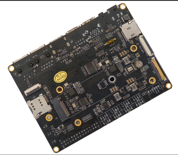
obverse
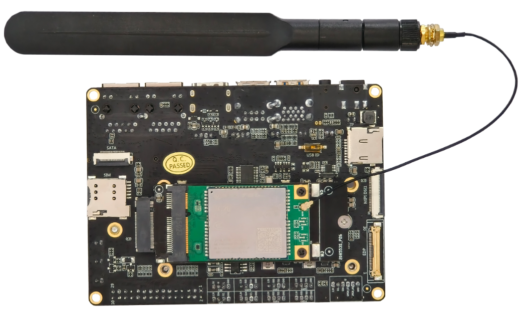
¶ Development board (including 4G module)

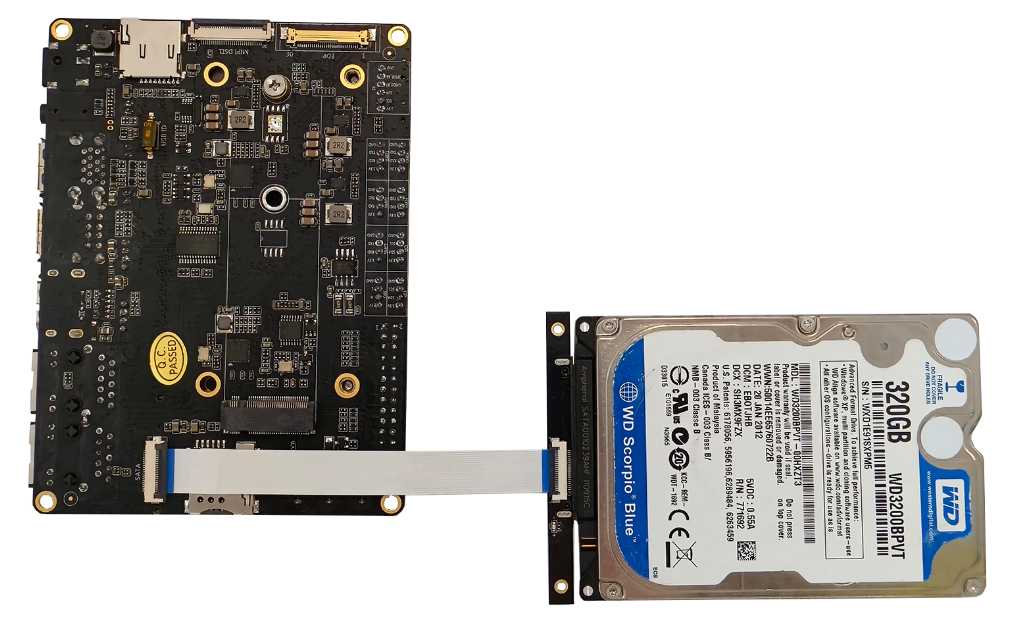
¶ Development board (including SATA)
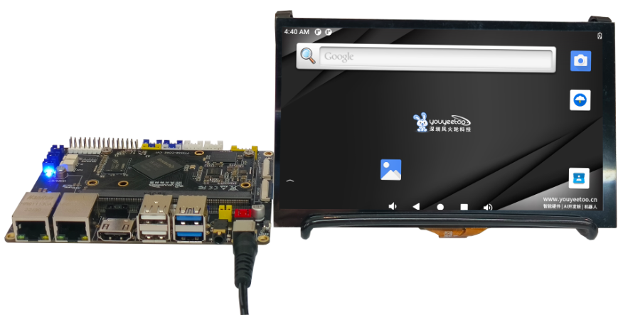
¶ Development board (including 7-inch screen)
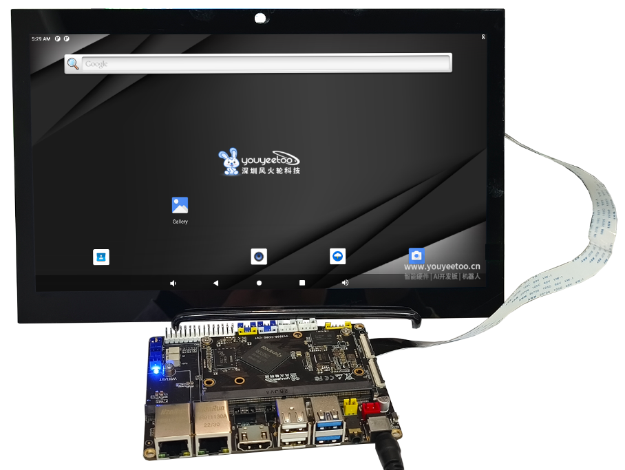
¶ Development board (including EDP screen)
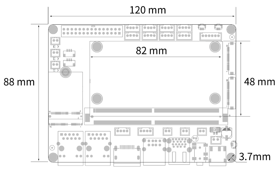
¶ Dimensional drawing
¶ interface
¶ YY3568 front interface diagram
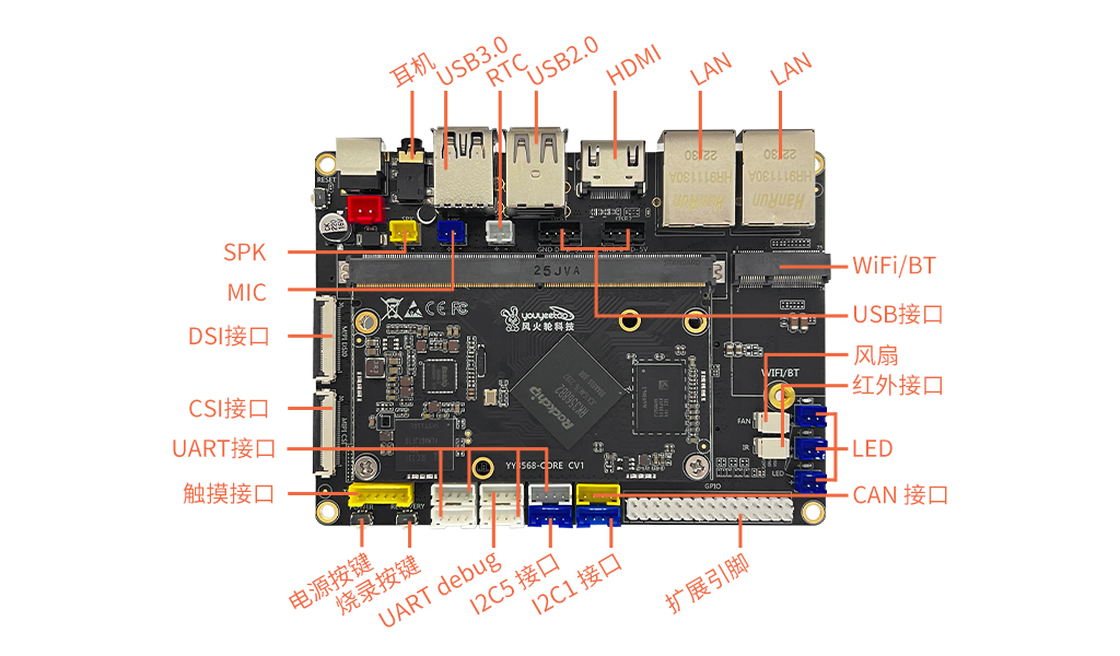
¶ YY3568 reverse interface diagram
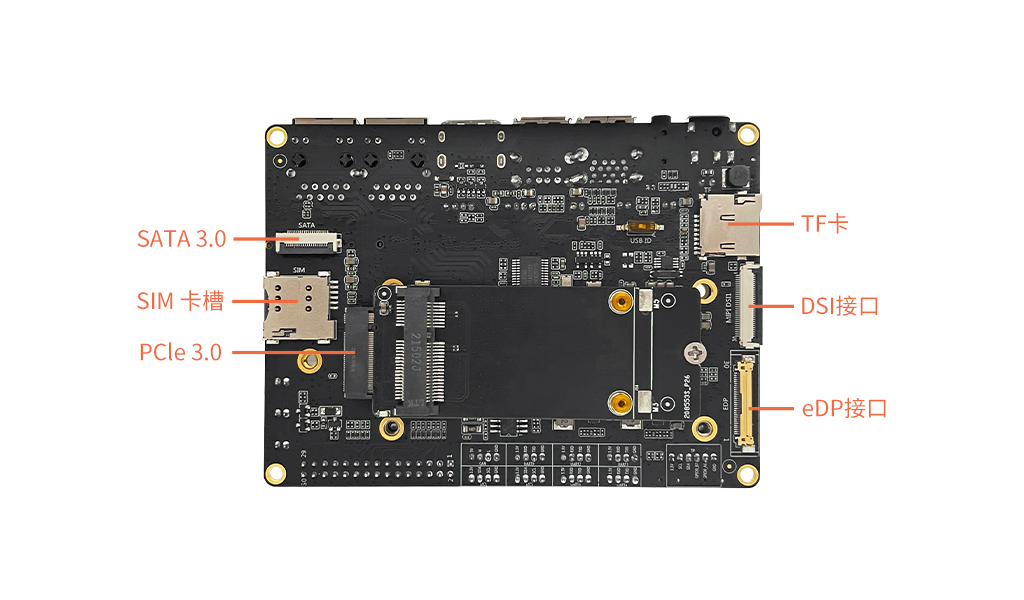
¶ Schematic
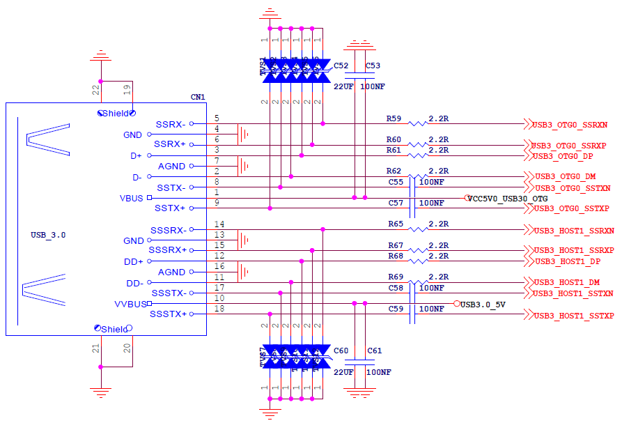
¶ USB3.0 circuit
The YY3568 development board leads to two usb3.0. USB supports maximum power (voltage 5V, current maximum 1A). The USB3.0 diagram is shown below:
The schematic diagram of USB3.0 is as follows:
¶ USB2.0 Host circuit
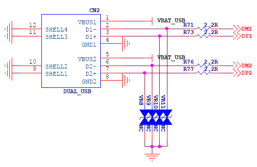
YY3568 development board leads to two usb2.0. USB supports maximum power (voltage 5V, current maximum 1A).
The schematic diagram of USB2.0 is shown in the figure below:
¶ Camera_mipi_csi circuit
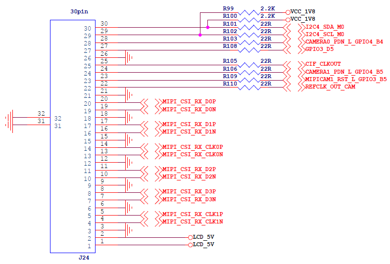
The YY3568 development board leads to the csi interface, which is adapted to the mipi csi camera of YY3568 Camera.
The schematic diagram of csi is as follows:
¶ HDMI circuit
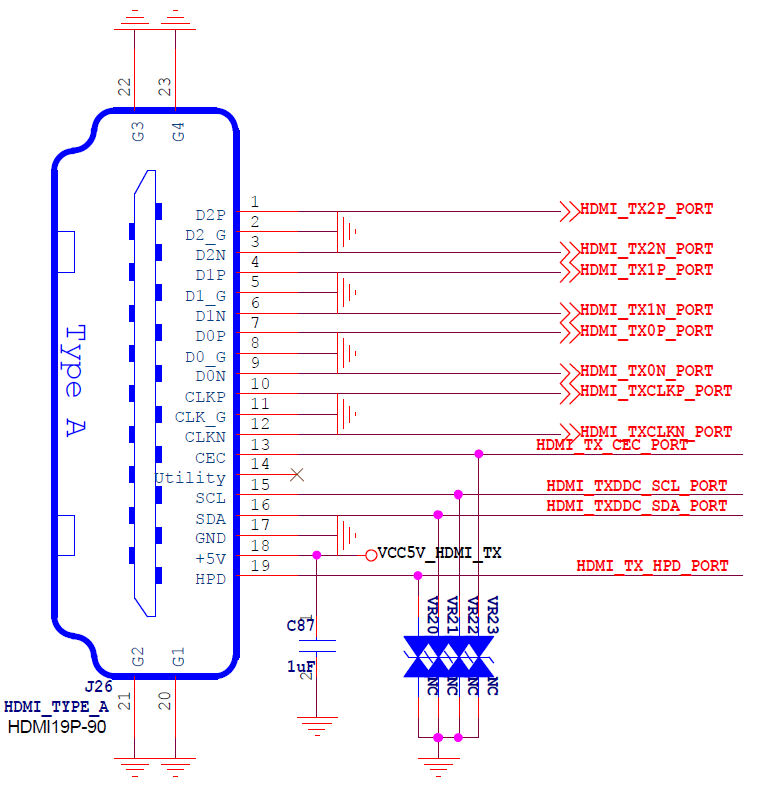
The HDMI interface of YY3568 development board supports HDMI2.0 protocol. The schematic diagram is as follows:
¶ DSI display circuit
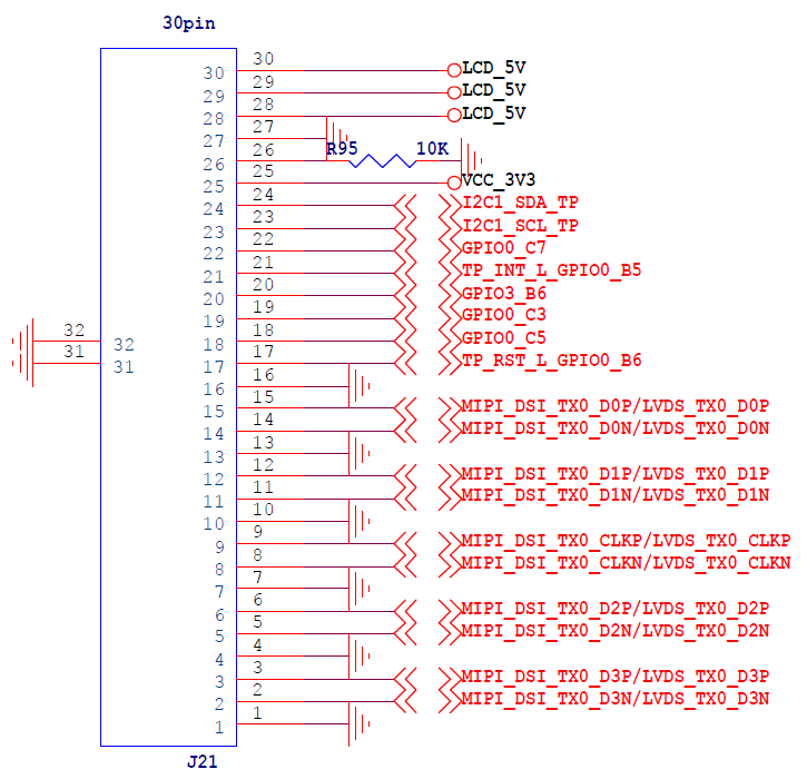
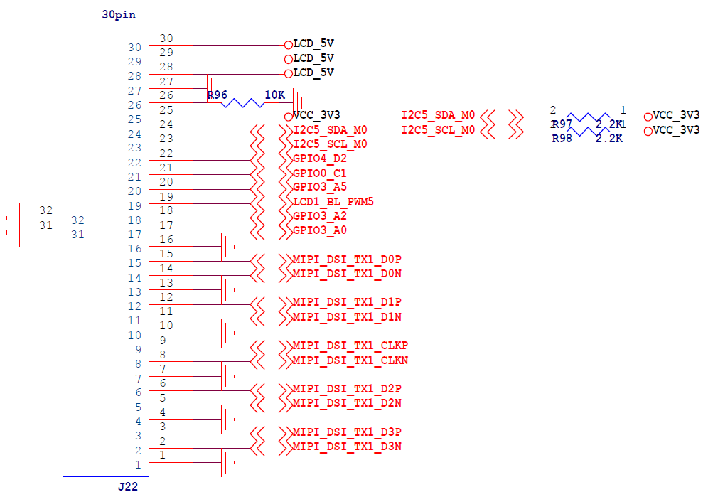
The DSI0 and DSI1 of the YY3568 development board cannot be used at the same time. If they must be used at the same time, the HDMI driver needs to be turned off. The DSI schematic diagram is as follows:
¶ EDP display circuit
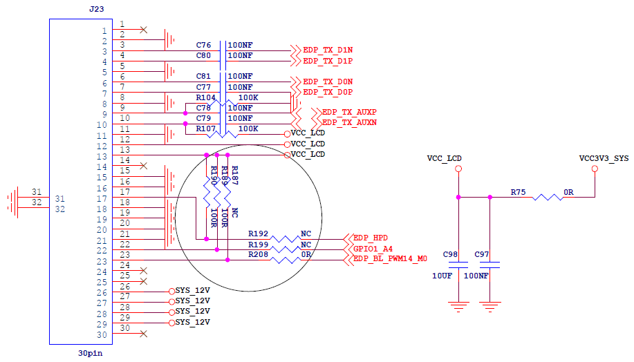
The EDP interface of the YY3568 development board conflicts with the DSI interface and cannot be used at the same time, only one of the two can be selected. The schematic diagram of EDP is as follows:
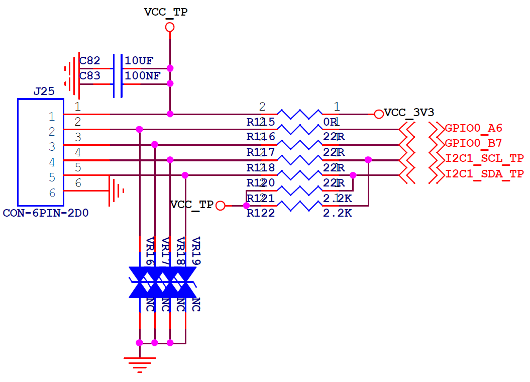
¶ TP touch circuit
The TP interface of the YY3568 development board is the touch interface of the 11.6-inch EDP screen. The TP schematic diagram is as follows:
¶ SPK (speaker) interface
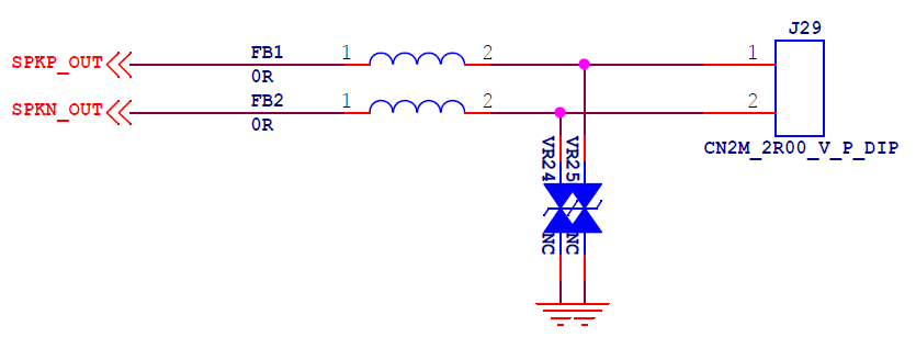
The YY3568 development board leads to an SPK interface, which can be connected to speaker equipment. The audio can be set to output from the SPK interface on the software. Among them SPK power (4 ohm 2W). The schematic diagram of SPK is as follows::
¶ MIC (microphone) interface
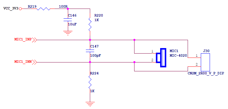
The MIC interface of YY3568 development board is positive and negative active. The schematic diagram of the MIC is as follows:
¶ Button circuit
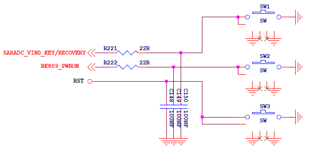
The three buttons on the YY3568 development board are reset button, programming button and power button. The schematic diagram of the button is as follows:
¶ WiFi and Bluetooth circuit
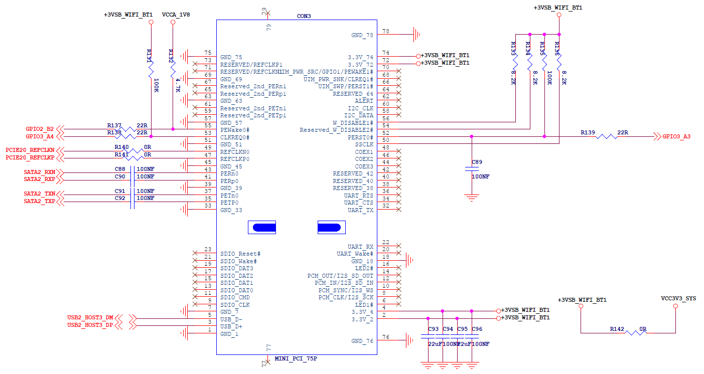
The M.2 interface of the YY3568 development board connected to WiFi is the same as the M.2 interface of SATA, so the functions of WiFi and SATA can only be selected from one of the two. The schematic diagram of the M.2 connected to WiFi and Bluetooth is as follows:
¶ TF card circuit
¶ PCIE circuit
¶ IR circuit
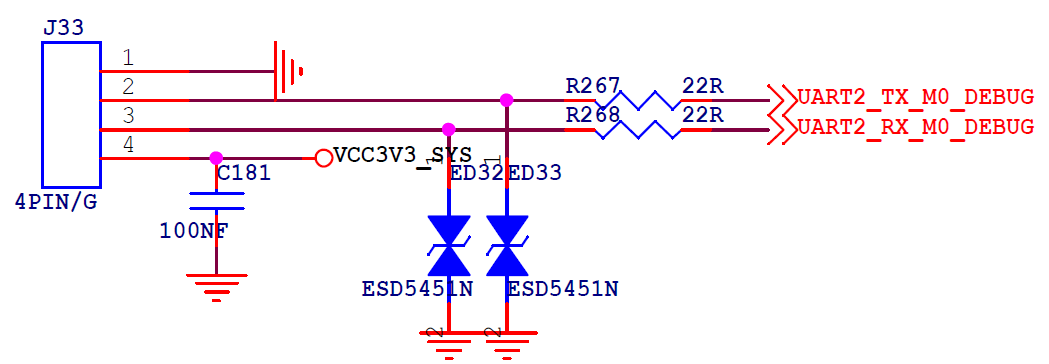
¶ Serial port debug circuit
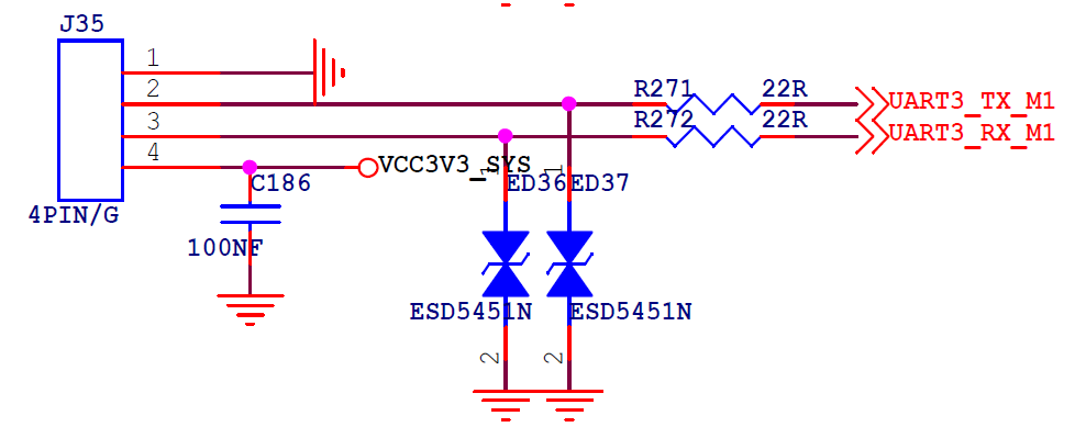
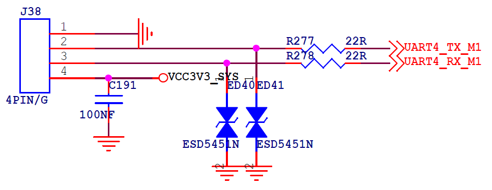
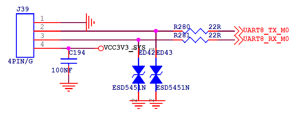
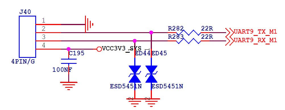
¶ Serial port circuit
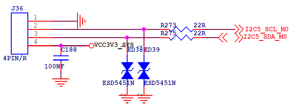
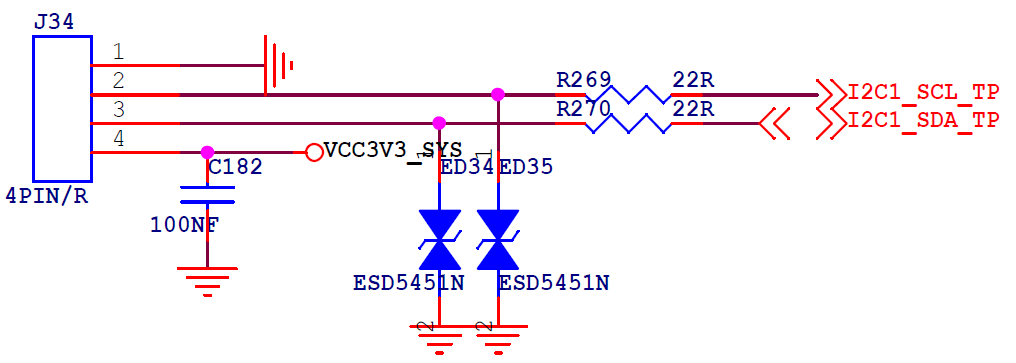
¶ IIC circuit
¶ CAN circuit

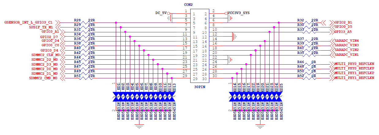
¶ Expansion circuit
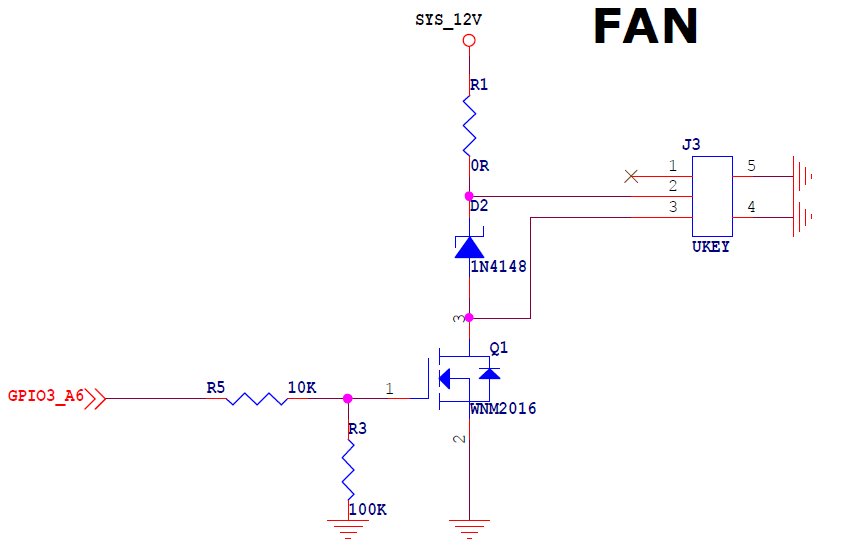
¶ FAN
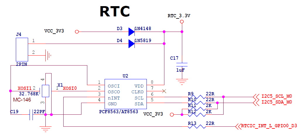
¶ RTC
