¶ NFC Call Experiment In Android
¶ Introduction to onboard NFC
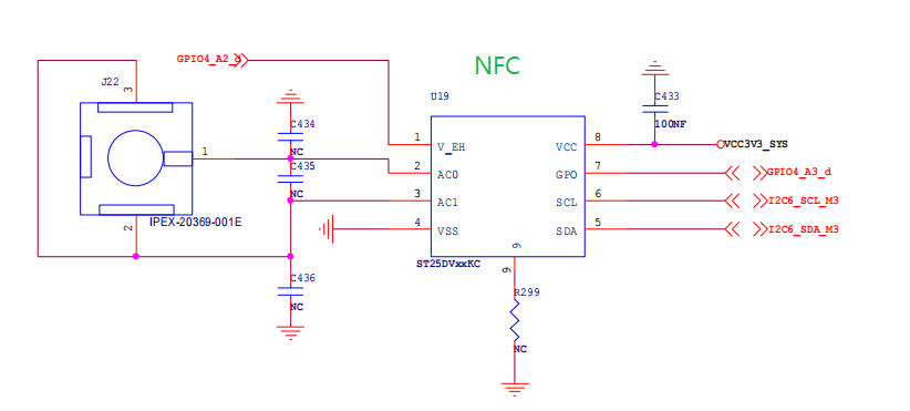
The onboard NFC chip uses ST25DV04KC semiconductor, as shown in the circuit diagram

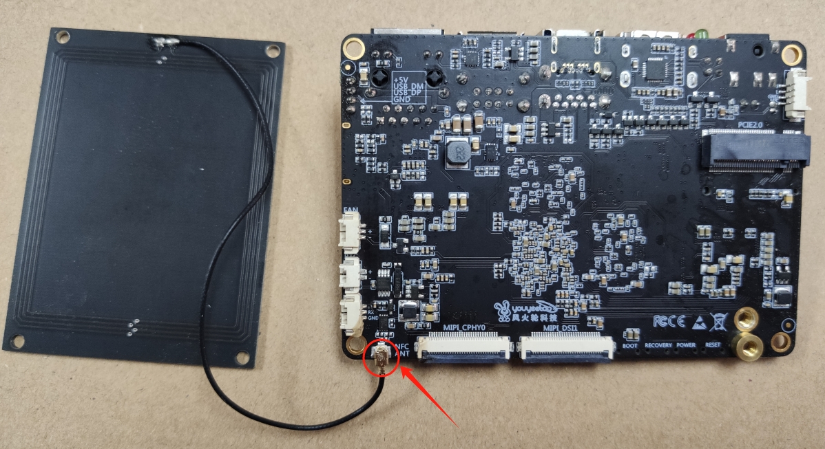
NFC antenna connection diagram:

¶ Experiment on NFC chip driven by I2C communication
To drive NFC, the first firmware version that needs to be refreshed is the version starting from 20240402. If your development board firmware version is newer than this, you don't need to upgrade it

- Firmware download link
Official Download
http://dd.youyeetoo.cn:5000/sharing/DjFERN0BC
Google Download
https://drive.google.com/drive/folders/1XBzTDFPYHVrS4fpvgbDufygP3sQRA31Q?usp=drive_link
Please refer to the burning system section for firmware flashing
Development board end control NFC corresponding APP
The development board is developed under the Android system and is mainly designed in two layers:
The JNI layer is responsible for I2C low-level communication and GPO interrupt monitoring
The Java layer is responsible for the implementation of various functional logic in ST25DV
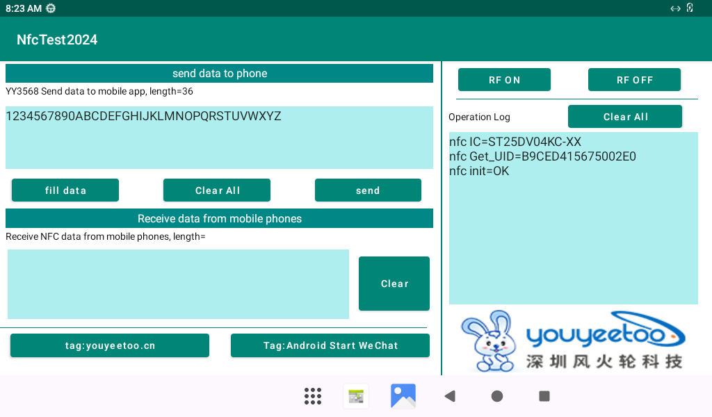
The implementation effect of the development board software is shown in the figure:

The upper left part of the interface is mainly used to send data from the development board to the mobile phone
Fill data: Fill in test data
Clear All: Clear
Send: The development board sends data to the phone
The lower left part of the interface is mainly used to receive messages from mobile phones
Clear: Clear the data sent by the phone
On the bottom left side of the interface: Write labels
Tag: youyeetoo.cn Write a label for www.youyeetoo.cn
Tag: Android Start WeChat Write tag: Enable the phone to flash the development board antenna and start the WeChat app automatically
On the right side of the interface: is the operation log of the operation section
RF ON: Enable RF wireless channel
RF OFF: Turn off RF wireless channel
The FTM data transmission process and protocol between the development board and the mobile phone are as follows:
1 sender -->receiver sends inquiry packets
FE FE FE  FE  FLG1 00 00 00 14 L1 L2 L3 L4 FF FF FF FF 45 4E 44
Among them
FLG1: indicates the direction of data transmission, 02 development board ->mobile, 03: mobile ->development board
L1 L2 L3 L4: Indicates the total length of data to be sent (including all query packet lengths+business data length): The high bit of L1 length, L4 is the lowest bit of length, L2, L3, and so on


2 receiving end -->sending end responds to the response packet
FE FE FE FE 04 00 00 00 00 14 FLG2 00 00 00 00 FF FF FF FF 45 4E 44
among
FLG2: Indicates whether data acceptance is allowed E7 indicates acceptance, while E9 indicates busy refusal
The process of sending data from the sender:
- The sender sends an inquiry packet first, asking if the target can accept the specified length of data
If the target response allows sending, proceed to step 3; otherwise, exit sending - Split and unpack the data and send it until it is complete
The process of receiving data at the receiving end: - Received a query to see if it is possible to accept a specified length packet. If it is allowed to send a reply packet, proceed to step 2. Otherwise, if it is busy, reject the reply packet to the sender and end the acceptance
Wait and receive the data in sequence until the specified length of data is received, and combine it into a complete package
Due to the large amount of code, it will not be displayed here. Please download the source code for viewing and verification
Development board app and source code download:
Compiled APK:
http://dd.youyeetoo.cn:5000/sharing/eYawgiQBv
Source code:
http://dd.youyeetoo.cn:5000/sharing/XN2kfOz3N
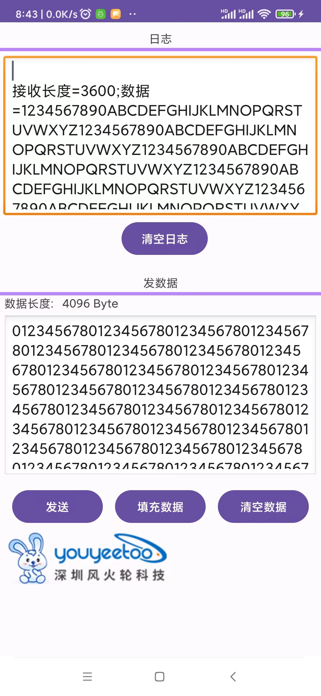
Mobile NFC corresponding APP
The mobile app refers to the development library provided by STMicroelectronics for secondary packaging development

Clear log: Clear the previous part of the log
Send: Send data from the mobile end to the development board
Fill in data: Fill in the data to be sent
Clear data: Clear the data to be sent
The FTM data transmission process and protocol between the development board and the mobile phone are the same as the above development board
Due to the large amount of code, it will not be displayed here. Please download the source code for viewing and verification
Mobile app and source code download:
Compiled APK:
http://dd.youyeetoo.cn:5000/sharing/CHmL7XtOo
Source code:
http://dd.youyeetoo.cn:5000/sharing/41oF789Vh